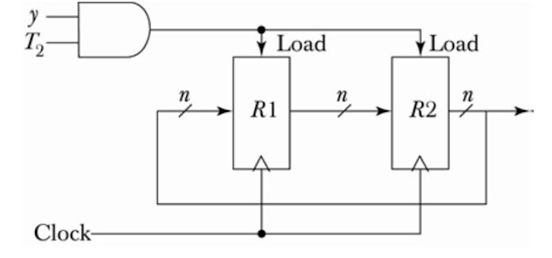
Show the block diagram of hardware that implements the following register transfer statement: yT2 : R1 R1, R1 R2
Q.) Show the block diagram of the hardware (Similar to fig. 4.2a) that implements the following register transfer statement:
yT2: R<-- R1, R1
<-- R2
Ans.)
Ø Here we have used AND gate because in the equation
we can see that both the input is in multiplication so we have to use the gate
accordingly
Ø The output from the AND gate is transferred to the
register R1 & R2 the data is transferred from R1 to R2 and from R2 to R1
Ø Both the register are connected to clock
